
The Union Cabinet in its weekly meeting held on Wednesday the 15th of July 2026 approved a 6-lane Greenfield Elevated Corridor covering over 46 kilometer between National Highway-19 and Varanasi Ring Road in Uttar Pradesh on Hybrid Annuity Model, improving urban mobility.
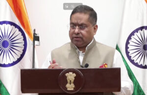
Briefing reporters after the Cabinet the Information and Broadcasting Minister Ashwini Vaishnaw said that the total capital cost of the project stands over 14 thousand 4 hundered crore rupees and will provide seamless connectivity between NH-19 and the Varanasi Ring Road, significantly decongesting the city’s road network and improving urban mobility.
It is expected to reduce the average travel time across the project influence area from approximately 60 minutes to 20 minutes.
Vaishnaw added that the project will significantly improve connectivity to major religious, educational and cultural landmarks.
The Union Cabinet has also approved development of around 43 kilometer 6 and 4 lane Elevated Corridor along Varuna River Bank in Uttar Pradesh at total Capital Cost of around 11 thousand crore rupees.
This corridor is a major component of the Varanasi Decongestion Plan and will provide seamless connectivity between NH-31 and Kashi Railway Station and is expected to improve access to Varanasi Ring Road, Varanasi Airport, Kashi Railway Station,Varanasi Junction, Deen Dayal Upadhyaya Junction.
The Cabinet has approved Semicon 2.0 programme with a budgetary outlay of 1 lakh 27 thousand 500 crore rupees to for the development of India’s semiconductor design and manufacturing ecosystem.
The I&B minister added that building on the momentum of Semicon 1.0, the scheme aims to further the government’s commitment to putting India on the global semiconductor map.
He said that the scheme will support economic growth, strengthen supply chain resilience, and establish technological leadership in critical sectors.
The minister said that Semicon 2.0 seeks to holistically build the semiconductor ecosystem through six pillars- Design, Machines and materials, Setting up more fabs, Further strengthening the ATMP-OSAT industry and Research and Development.
Vaishnaw said that in Semicon 1.0 programme, the focus was on starting and establishing the industry and Under Semicon 2.0, the chips required for all our strategic needs will be designed in India, and by the end of this semiconductor programme,the country will become self-reliant in chip design.
Given the growing global interest in India’s semiconductor programme, every major industry leader wants to establish a presence in the country, Vaishnaw added stating that India has already forged partnerships with the US, Japan, the EU, the Netherlands, Singapore, and Germany.
The Cabinet also approved the Mobile Phone Manufacturing Scheme ((MPMS) with a budgetary outlay of 62 thousand 500 crore rupees to be implemented for the next 5 years.
The scheme will provide incentive support of 2.25 percent to 5 percent on eligible sales for manufacturing mobile phones in the country.
The minister said that an additional incentive of up to 1.5 percent is linked to domestic sourcing of key components and sub-assemblies.
He said the scheme is expected to generate cumulative mobile phone production of approximately 39 lakh crore rupees during its tenure, while the cumulative exports are expected to increase from approximately 7.5 lakh crore rupees to 15 lakh crore rupees.
Vaishnaw informed that the scheme is also expected to create around 60 thousand direct jobs.